What is a multi-layer PCB?
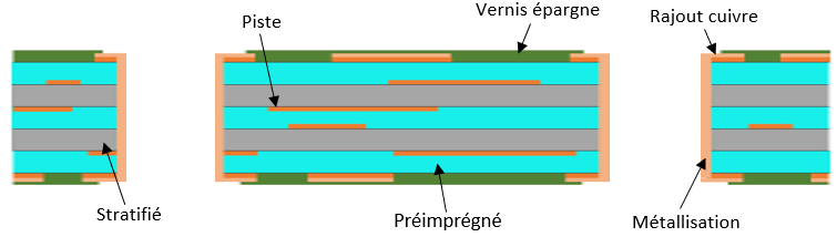
The multilayer PCB is composed of several etched layers (called internal layers), which are stacked and hot pressed with prepregs (epoxy glue). This process is followed by copper reinforcement and plating to ensure the connection of all internal and external faces of the PCB.
Multi-layer diagram
Example of a six-layer board:
Examples of use:
- GPS system
- Medical
- Aerospace
- Scientific equipment
- Defence
- Aeronautics
- Atomic accelerators
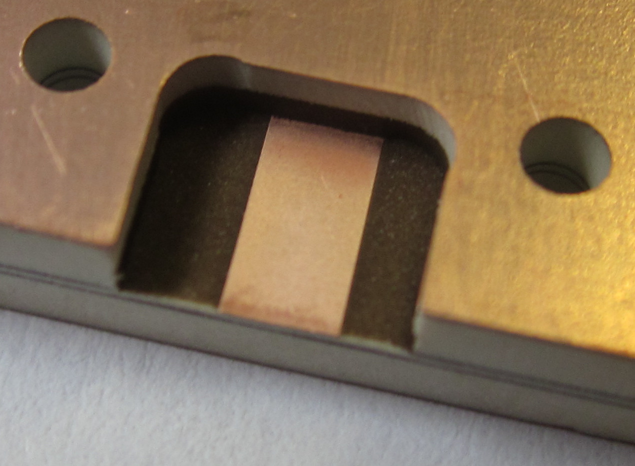
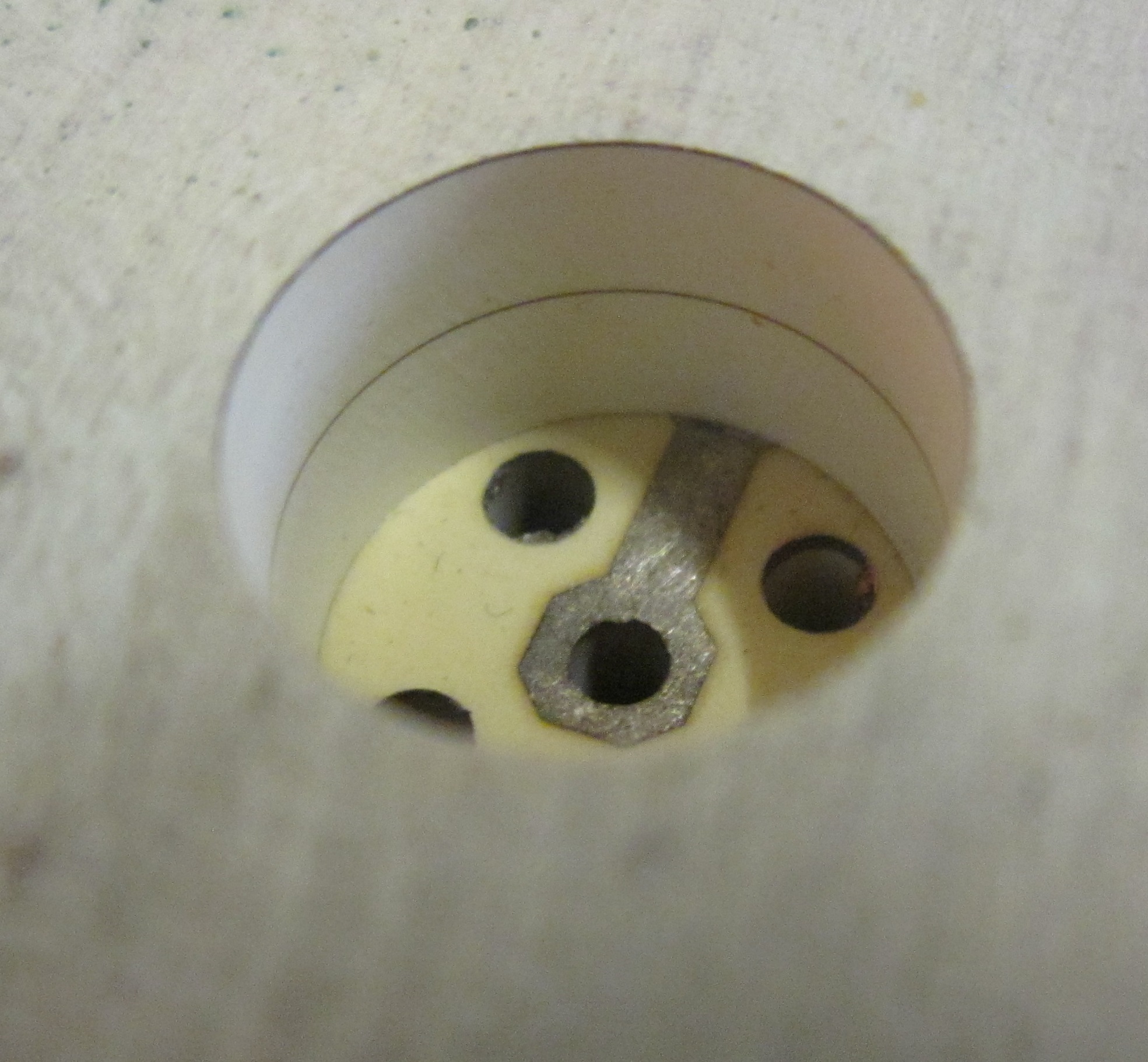
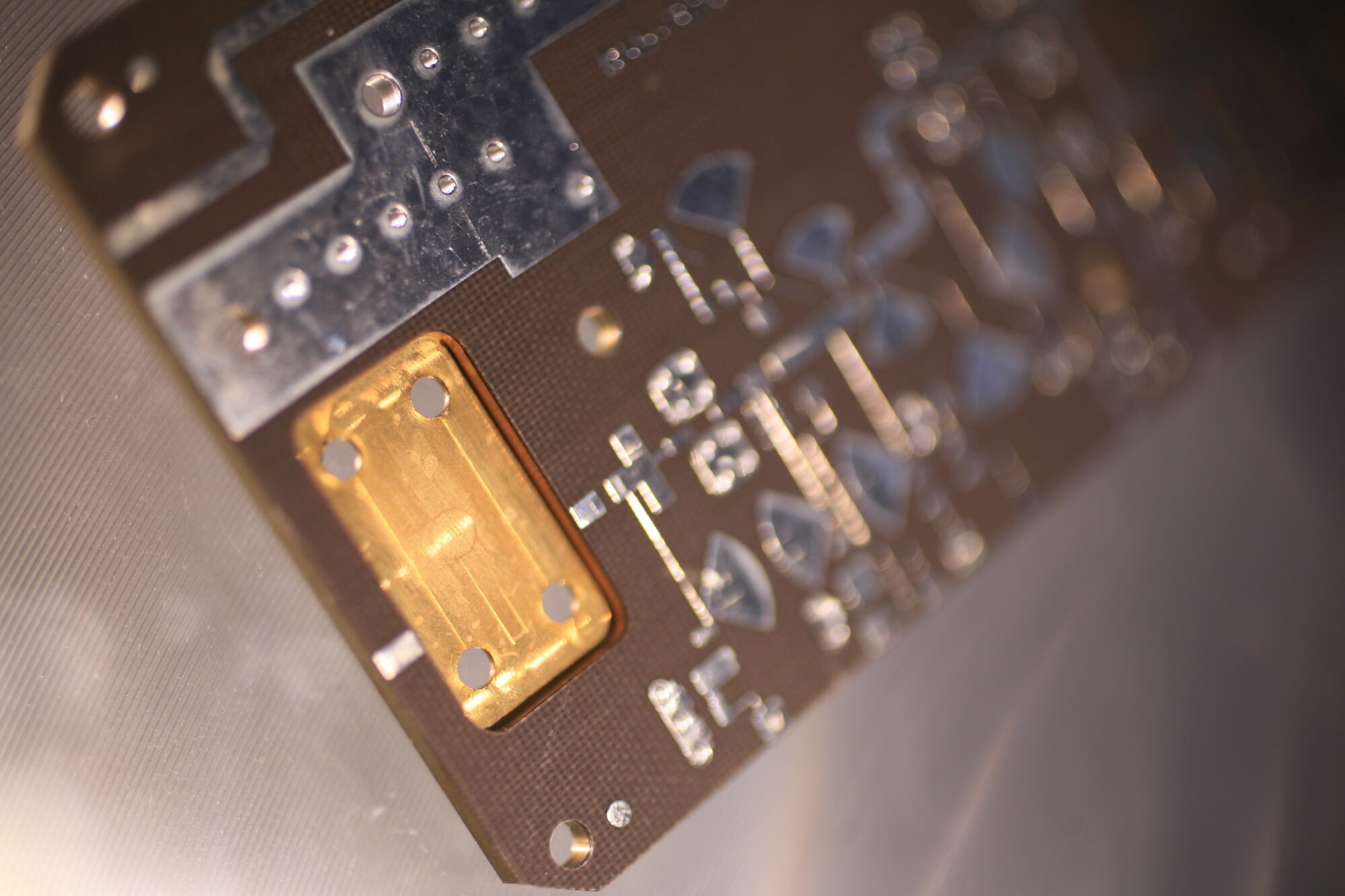
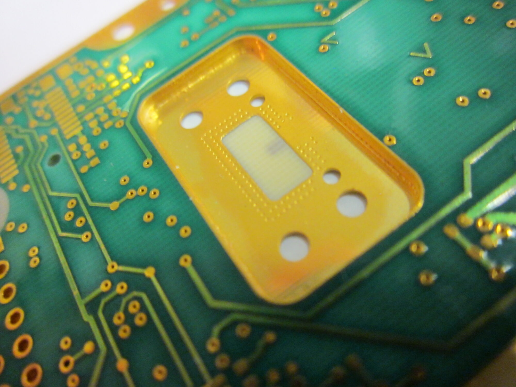
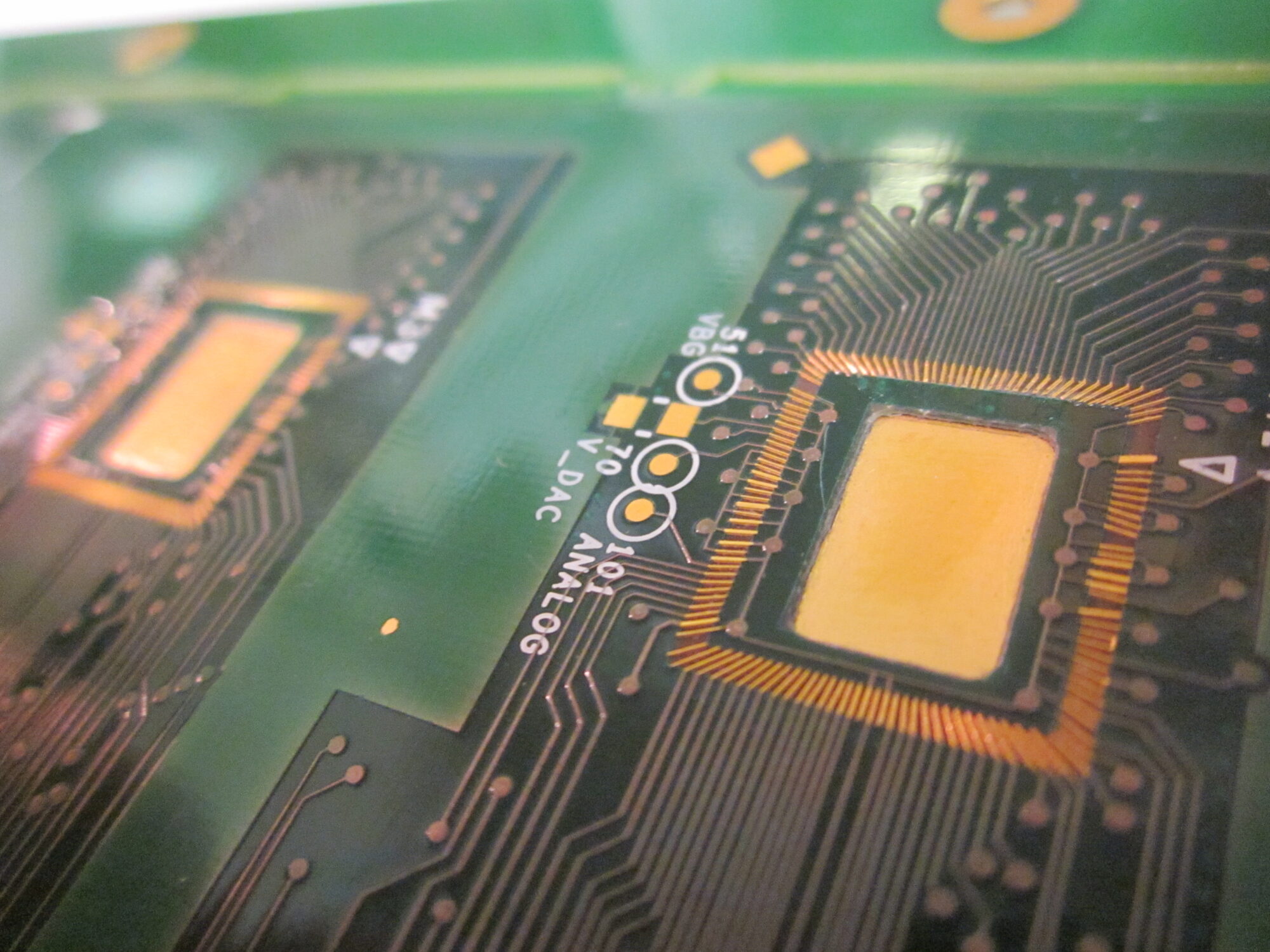
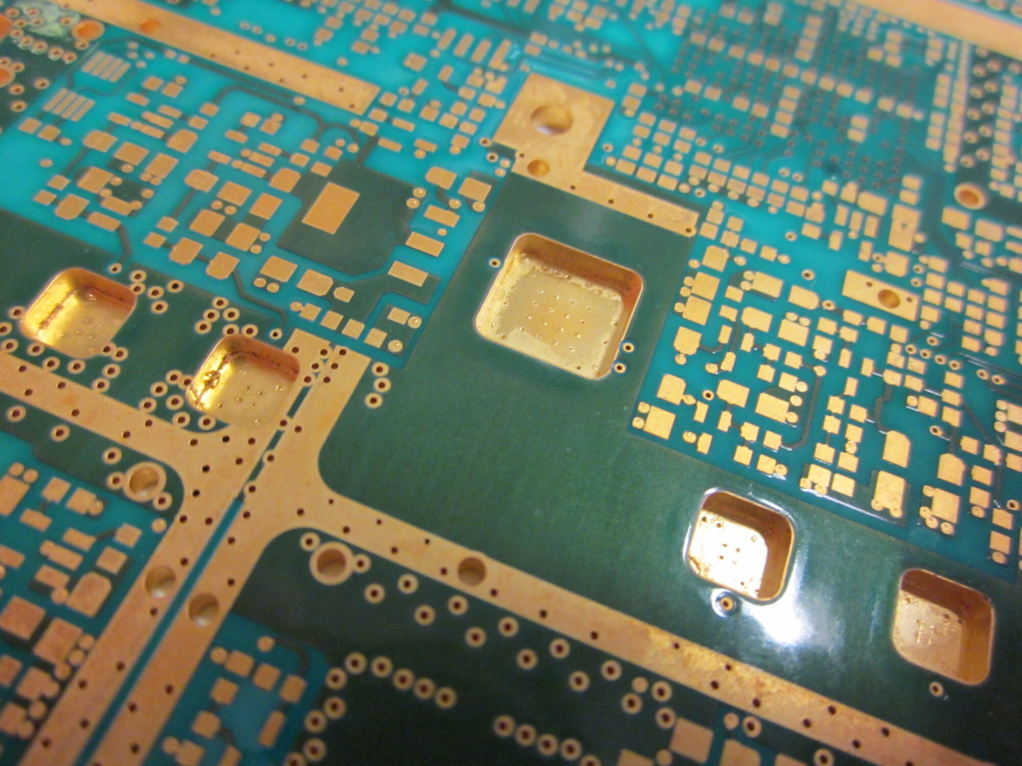
Examples of implementation with cavities
- PCB edge with PTFE coated access line
- Non-plated cavity for coaxial cable access
- Non-plated walls
- Plated wall cavity with image and hole at the bottom of the cavity
- Cavity for housing a component connected by wire bonding
- Plated wafer cavity
For further information, please contact us
 Attention, vous utilisez un navigateur peu sûr !