HDI
What is a HDI?
UAn HDI PCB is defined by its high density of interconnections. HDI PCBs have thin traces and isolations, vias and microvias.
What is a buried hole?
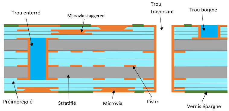
A buried hole is a hole between several internal layers. Buried holes are usually drilled mechanically. (see HDI diagram)
What is a blind hole?
A blind hole only goes through part of the PCB, it is a non-through hole. The blind hole is made by mechanical or laser drilling. (see HDI diagram)
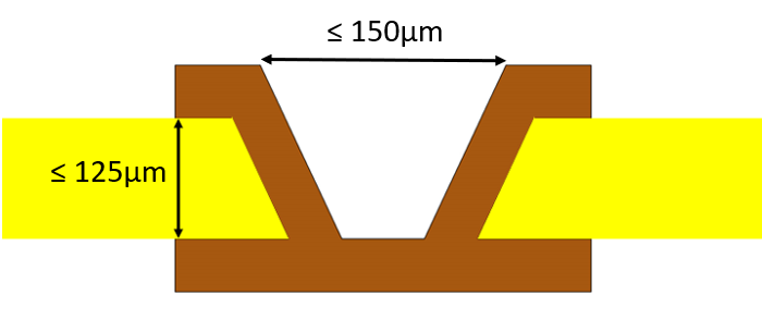
What is a microvia?
LeMicrovias are blind holes drilled with lasers. In most cases, a microvia is a blind hole with a diameter of 150µm or less and a height no greater than its width. The metal plating ratio of the microvia is usually 0.8 to 1.
SBU Definition
Sequential Build Up (SBU) technology is a technology used to create HDI circuits. This technology combines several successive layers in a sequence of holes. It uses buried, blind and microvias technologies to densify the interconnections.
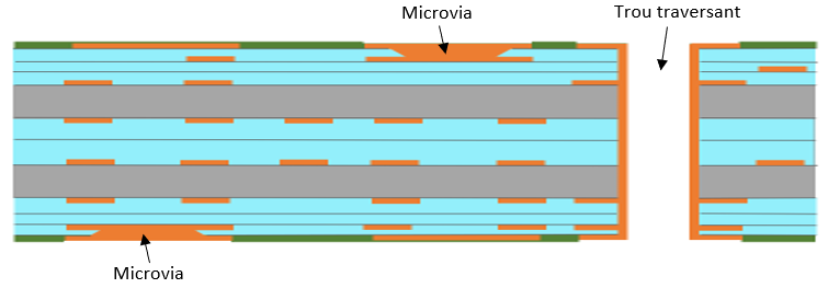
Types of HDI features
Case I
It includes:
- Metal plated microvias (copper filled or not according to the request) and metal plated through-hole for interconnection
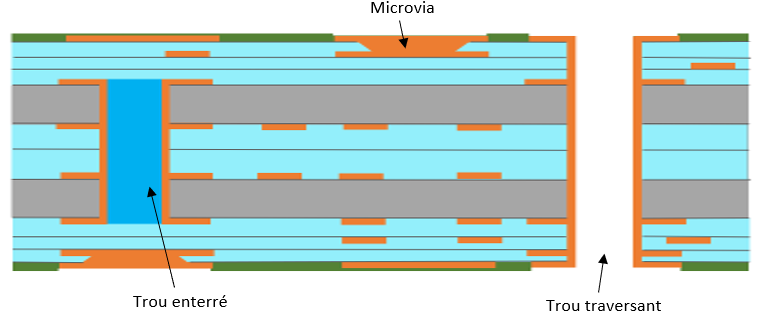
Case II
IIt includes:
- Metal plated microvias (copper filled or not according to the request) and metal plated through-hole for interconnection
- Buried holes
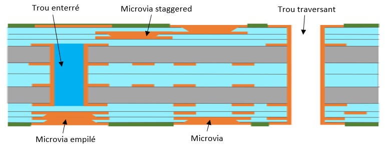
Case III
It includes:
- Metal plated microvias (copper filled or not according to the request) and metal plated through-hole for interconnection
- Buried holes
- Staggered or stacked microvias
Staggered holes may or may not be filled with copper, while stacked holes are necessarily filled with copper.
HDI diagram
Examples of use:
- Automotive
- Smartphones and tablets
- Defence and aeronautics
- Medical
- Laptop computer
- Railway
- Aerospace
For further information, please contact us
 Attention, vous utilisez un navigateur peu sûr !